- 您现在的位置:买卖IC网 > Sheet目录1991 > CS5509-ASZR (Cirrus Logic Inc)IC ADC 16BIT SGL SUPP 16-SOIC
CS5509
2
DS125F3
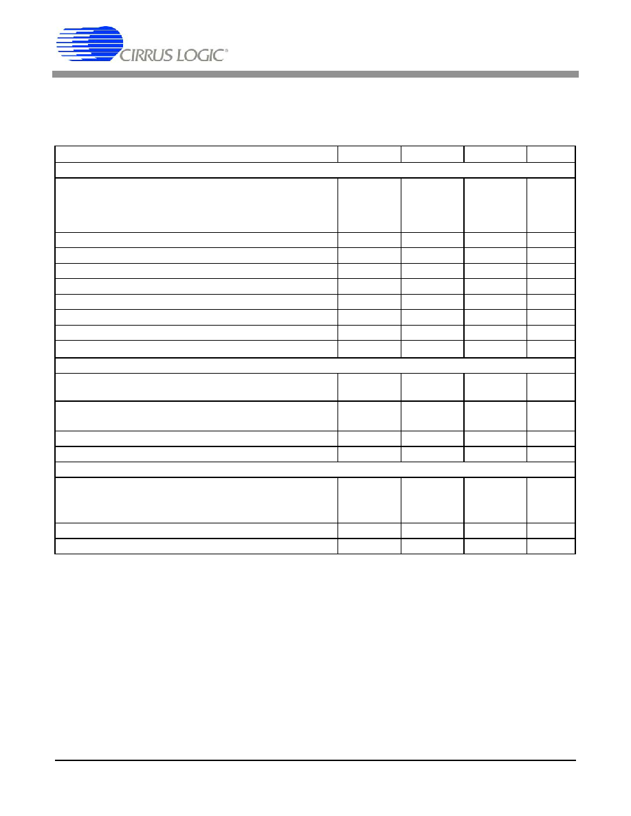
Notes: 1. Both source resistance and shunt capacitance are critical in determining the CS5509's source
impedance requirements. Refer to the text section Analog Input Impedance Considerations.
2. Specifications guaranteed by design, characterization and/or test.
3. Applies after calibration at the temperature of interest.
4. Total drift over the specified temperature range since calibration at power-up at 25 °C.
5. The input is differential. Therefore, GND
≤ Signal + Common Mode Voltage ≤ VA+.
6. The CS5509 can accept input voltages up to the VA+ analog supply. In unipolar mode the CS5509 will
output all 1's if the dc input magnitude ((AIN+) - (AIN-)) exceeds ((VREF+) - (VREF-)) and will output all
0's if the input becomes more negative than 0 Volts. In bipolar mode the CS5509 will output all 1's if the
dc input magnitude ((AIN+) - (AIN-)) exceeds ((VREF+) - (VREF-)) and will output all 0's if the input
becomes more negative in magnitude than -((VREF+) - (VREF-)).
7. All outputs unloaded. All inputs CMOS levels.
* Refer to the Specification Definitions immediately following the Pin Description Section.
ANALOG CHARACTERISTICS (T
A = 25 °C; VA+ = 5V ±5%; VD+ = 3.3V ±5%; VREF+ = 2.5V,
VREF- = 0V; fCLK = 32.768 kHz; Bipolar Mode; Rsource = 40 Ω with a 10 nF to GND at AIN; AIN- = 2.5V; unless oth-
Parameter*
Min
Typ
Max
Unit
Accuracy
Linearity Error
fCLK = 32.768 kHz
fCLK = 165 kHz
fCLK = 247.5 kHz
fCLK = 330 kHz
-
0.0015
0.005
0.003
0.0125
± %FS
Differential Nonlinearity
-
±0.25
±0.5
LSB
Full-scale Error
(Note 3)
-
±0.25
±2
LSB
Full-scale Drift
(Note 4)
-
±0.5
-
LSB
Unipolar Offset
(Note 3)
-
±0.5
±2
LSB
Unipolar Offset Drift
(Note 4)
-
±0.5
-
LSB
Bipolar Offset
(Note 3)
-
±0.25
±1
LSB
Bipolar Offset Drift
(Note 4)
-
±0.25
-
LSB
Noise (Referred to Output)
-
0.16
-
LSBrms
Analog Input
Analog Input Range
Unipolar
Bipolar
-
0 to +2.5
±2.5
-
V
Common Mode Rejection
dc
fCLK = 32.768 kHz
50, 60 Hz
(Note 2)
-
120
105
-
dB
Input Capacitance
-
15
-
pF
DC Bias Current
(Note 1)
-
5
-
nA
Power Supplies
DC Power Supply Currents
ITotal
IAnalog
IDigital
-
350
300
60
450
-
A
Power Dissipation
(Note 7)
-
1.7
2.25
mW
Power Supply Rejection
-
80
-
dB
发布紧急采购,3分钟左右您将得到回复。
相关PDF资料
CS5512-BSZ
IC ADC 20BIT EXTERNAL OSC 8-SOIC
CS5526-BSZR
IC ADC 20BIT W/4BIT LATCH 20SSOP
CS5528-ASZR
IC ADC 24BIT 8CH 24-SSOP
CS5529-ASZR
IC ADC 16BIT W/6BIT LATCH 20SSOP
CS5530-ISZR
IC ADC 24BIT 1CH W/LNA 20-SSOP
CS5534-ASZR
IC ADC 24BIT 4CH W/LNA 24-SSOP
CS5534-BSZR
IC ADC 24BIT 4CH W/LNA 24SSOP
CS5550-ISZR
IC ADC 2CH LOW-COST 24-SSOP
相关代理商/技术参数
CS5510
制造商:CIRRUS 制造商全称:Cirrus Logic 功能描述:16-bit and 20-bit, 8-pin ΔΣ ADCs
CS5510_09
制造商:CIRRUS 制造商全称:Cirrus Logic 功能描述:16-bit and 20-bit, 8-pin ΔΣ ADCs
CS5510-AS
功能描述:模数转换器 - ADC 16-Bit Delta Sigma ADC Ext. OSC RoHS:否 制造商:Texas Instruments 通道数量:2 结构:Sigma-Delta 转换速率:125 SPs to 8 KSPs 分辨率:24 bit 输入类型:Differential 信噪比:107 dB 接口类型:SPI 工作电源电压:1.7 V to 3.6 V, 2.7 V to 5.25 V 最大工作温度:+ 85 C 安装风格:SMD/SMT 封装 / 箱体:VQFN-32
CS5510-ASR
功能描述:模数转换器 - ADC IC 16-Bit 8-Pin Delta Sigma ADC RoHS:否 制造商:Texas Instruments 通道数量:2 结构:Sigma-Delta 转换速率:125 SPs to 8 KSPs 分辨率:24 bit 输入类型:Differential 信噪比:107 dB 接口类型:SPI 工作电源电压:1.7 V to 3.6 V, 2.7 V to 5.25 V 最大工作温度:+ 85 C 安装风格:SMD/SMT 封装 / 箱体:VQFN-32
CS5510-ASZ
功能描述:模数转换器 - ADC 16-Bit Delta Sigma ADC Ext. OSC RoHS:否 制造商:Texas Instruments 通道数量:2 结构:Sigma-Delta 转换速率:125 SPs to 8 KSPs 分辨率:24 bit 输入类型:Differential 信噪比:107 dB 接口类型:SPI 工作电源电压:1.7 V to 3.6 V, 2.7 V to 5.25 V 最大工作温度:+ 85 C 安装风格:SMD/SMT 封装 / 箱体:VQFN-32
CS5510-ASZ
制造商:Cirrus Logic 功能描述:A/D Converter (A-D) IC
CS5510-ASZR
功能描述:模数转换器 - ADC IC 16-Bit 8-Pin Delta Sigma ADC RoHS:否 制造商:Texas Instruments 通道数量:2 结构:Sigma-Delta 转换速率:125 SPs to 8 KSPs 分辨率:24 bit 输入类型:Differential 信噪比:107 dB 接口类型:SPI 工作电源电压:1.7 V to 3.6 V, 2.7 V to 5.25 V 最大工作温度:+ 85 C 安装风格:SMD/SMT 封装 / 箱体:VQFN-32
CS5511
制造商:CIRRUS 制造商全称:Cirrus Logic 功能描述:16-bit and 20-bit, 8-pin ΔΣ ADCs